


Articles / insights / PFAS / Sustainability / Water technology
Why the Semiconductor Industry Depends on PFAS
Why the Semiconductor Industry Depends on PFAS
October 16, 2026
Why the Semiconductor Industry Depends on PFAS
In the realm of modern technology, semiconductors are powering everything from smartphones to space shuttles. These tiny chips are the backbone of the digital age, enabling the functioning of countless devices. However, beneath their sleek exterior lies a complex manufacturing process that relies on a group of chemicals known as per- and polyfluoroalkyl substances (PFAS), often dubbed “forever chemicals” due to their persistence in the environment.

The semiconductor manufacturing process is highly complex and requires materials that can withstand intense conditions.
The Role of Semiconductors
Semiconductors are materials that have electrical conductivity between that of a conductor and an insulator. They are crucial in creating integrated circuits, which are essential for electronic devices. The global demand for semiconductors is immense, with the industry continually striving for smaller, faster, and more efficient chips to meet the ever-growing needs of technology.
Understanding PFAS
PFAS are a large group of human-made chemicals characterised by their strong carbon-fluorine bonds, which make them resistant to water, oil, and heat. This resistance is what makes them so valuable in industrial applications, but it also contributes to their persistence in the environment and potential health risks. PFAS have been used since the 1940s in various products, from non-stick cookware to firefighting foams, and more recently, they have become integral to semiconductor manufacturing.
Why the Chip Industry Relies on PFAS
The semiconductor manufacturing process is highly complex and requires materials that can withstand intense conditions. PFAS are used at various stages of this process due to their unique properties:
- Photolithography: This is a crucial step in semiconductor manufacturing where intricate patterns are etched onto silicon wafers. PFAS are used in photoresists and anti-reflective coatings, providing the precision needed for creating tiny circuits.
- Etching and Cleaning: PFAS compounds are employed in the etching process to create the required patterns on the wafer surface. They are also used in cleaning solutions to remove residues without damaging the delicate circuits.
- Heat Resistance: The high thermal stability of PFAS makes them ideal for applications that involve high temperatures, ensuring that materials do not degrade during the manufacturing process.
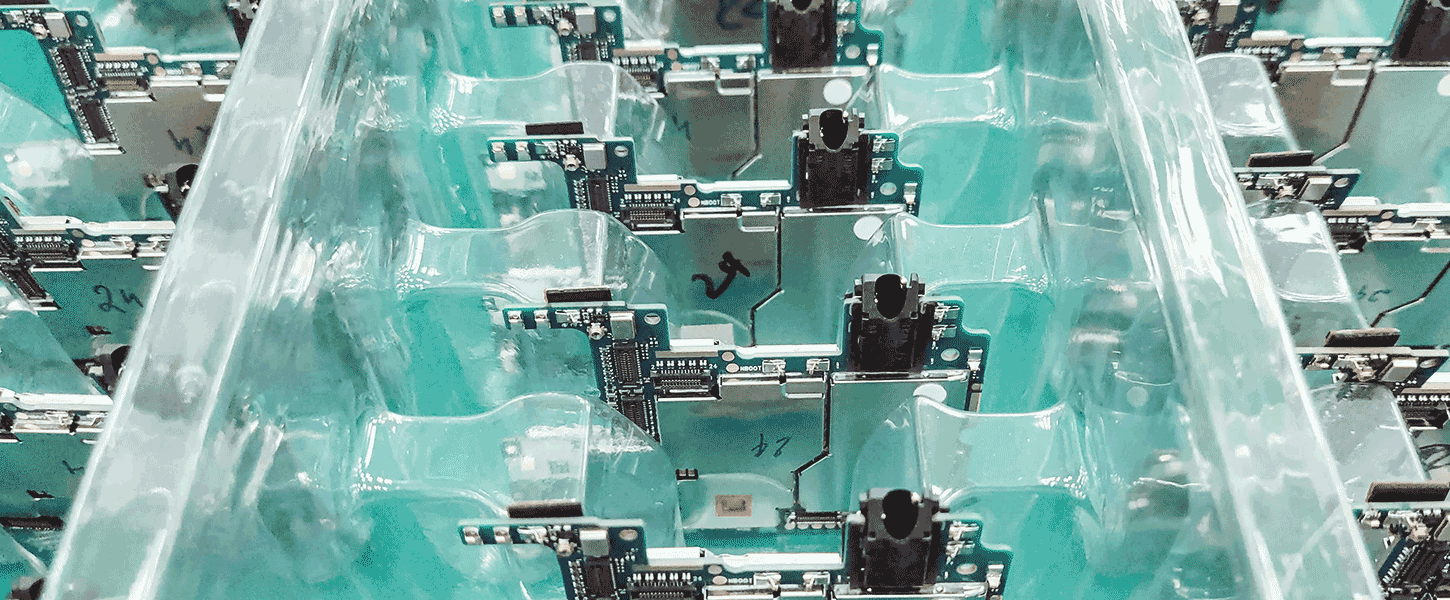
The semiconductor industry's reliance on PFAS presents a complex challenge.
Environmental and Health Concerns
While PFAS are invaluable to the semiconductor industry, their environmental and health implications cannot be overlooked. These chemicals are incredibly persistent, breaking down very slowly in the environment. As a result, they have been found in water supplies, wildlife, and even in human blood.
Research has linked PFAS exposure to various health issues, including hormonal disruptions, immune system effects, and an increased risk of certain cancers. This has led to growing concerns and regulatory scrutiny over their use and disposal.
The Path Forward: Balancing Innovation and Sustainability
The semiconductor industry’s reliance on PFAS presents a complex challenge; balancing technological advancements with environmental responsibility. Companies are investing in research to develop alternative materials that can match the performance of PFAS without the associated risks. Innovations in “green chemistry” are being explored to create sustainable solutions for semiconductor manufacturing.
Governments and industry leaders are also working together to establish regulations that limit PFAS emissions and encourage safer disposal practices. This includes setting strict guidelines for PFAS levels in water supplies and investing in new purification technologies.
How Arvia Can Help
Cleaning wastewater from a semiconductor fabrication plant is not a one-step process. There are many types of contaminants to deal with, which need to be removed to below the level of detection. It is a specialist job, from a careful understanding of the waste streams, to smart sensors for segregating streams, to optimise waste management and treatment.
Arvia’s water treatment processes, Nyex™ Ellenox and Rosalox are extremely effective in removing toxic contaminants such corrosion, solvents, and organic contaminants to below the level of detection. Arvia also offers an innovative approach to PFAS removal that is both effective and sustainable. Unlike conventional methods that generate secondary waste, their Nyex™ Florenox technology efficiently destroys PFAS, ensuring complete removal from wastewater.
Conclusion
Semiconductors and PFAS are intrinsically linked in a relationship that underscores the complexities of modern technology. As the demand for ever more sophisticated electronic devices grows, the challenge is to ensure that the chip industry can continue to innovate while minimising environmental impacts. The path forward will require collaboration across industries, governments, and environmental groups to develop solutions that safeguard both technological progress and the health of our planet. By doing so, we can ensure that the digital age is both bright and sustainable for generations to come.
More featured articles
04.17.2025

In this article we discuss PFAS and the implications of these forever chemicals on human and animal health. We examine the routes of exposure, health impacts and how Arvia is helping to tackle the PFAS problem.
03.27.2025

Press Release - Arvia Technology Launches Proven PFAS Destruction Solution
03.24.2025

In this article we discuss PFAS regulations, why regulation is necessary and the impact on industry and consumers.
Our wastewater treatment expertise
Our water technology can be used to treat a variety of water treatment applications. Once we understand the nature of your wastewater and your final water quality target, our water treatment specialists can make recommendations as to how best to treat your water. Take a look at some of the Nyex applications here:
Need help? Speak with an expert

